

Implant P+ Impurities: CMOS Processing (Part 5)
| Index | Chapter1 | Chapter2 | Chapter3 | Chapter4 |
| Digital Background | Semiconductor Background | CMOS Processing |
| 3.1 | 3.2 | 3.3 | 3.4 | 3.5 | 3.6 |
| Fabrication Steps | Create N-Well and Field Oxide | Create Gate Oxide and Poly Layer | Implant N+ Impurities | Implant P+ Impurities | Create Metal Contact |
Just to remind you that the complete CMOS fabrication process, we are not discussing in a single post. Complete CMOS fabrication, I have divided into different Article as per above table.
Let’s start where we have left in the last post (3D view of the wafer).
Few things are important (Few points are just copy paste from the previous post for better understanding.:) )
- This is the ideal process. In actual fabrication the Gate Length is affected. I have explained that in the last post. Please refer that.
- We are going to add Boron as part of P+ impurities. We can add other also.
- As a part of side effect of this process, resistance of poly decreases, Pfet threshold affected. But we are not going to discuss all these in this post.
- NMOS needs a body contact (which will be of p+ doping) the same as the Source(GND)
- PMOS needs a body contact (which will be of n+ doping) the same as the Drain (Vdd)
- From process and steps point of view, there is no difference while creating the NMOS and PMOS devices (except mask and the impurities). So we can interchange the steps (Means First we can create PMOS and then NMOS).
- In this we are going to create PMOS (Source and Drain) only. We are not creating the NMOS body contact (just because of space issue in the diagram) but the concept remains same as in case of PMOS body contact as we have discussed in the previous post.

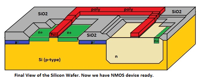
Final 3D view of the Silicon Wafer is:

Till now we have created
- Nwell
- Active Region
- Channel Stop Region
- Field Oxide.
- Gate Oxide
- Poly layer.
- N+ regions (Source and Drain) for NMOS device.
- P+ regions (Source and Drain) for PMOS device.
In the next post we will talk about adding Metal Contact which will help us to pass the signal or data to MOS devices from the other MOS devices or from the External world.

Thank you for sharing, this is nice presentation, very informative......
ReplyDeleteThere are number of mistakes in this presentation. The thick oxide is deposited not grown or the polysilicon would be consumed. The photoresist is specified as positive but the next figure shows it being removed in the shadowed area of the mask which would make it a negative acting resist. Positive resist is usually developed in a base solution not an acid and it is removed with a solvent (or an oxygen plasma. Boron implant is across the whole wafer as is shown in the etch diagram not just around the opening in the resist. There are better sources of information than this.
ReplyDeleteLooks like few of the items are for understanding purpose. Like Boron implant - It's not going to effect the rest of the area - so it's been shown only for a specific area (for understanding purpose, it's okay). Regarding Acid and solvent, it's been mentioned in one of the previous article that use some solution ( and it's just pointer/reference).
DeleteHi Both of you,
DeleteThanks a lot for correcting the mistakes. Thanks for reviewing this thoroughly. I have made few changes. Few things are just for the reference and understanding purpose. Obviously - you can't use this material for real fabrication purpose.
Thanks
Do you forget the RTP step to activate the dopants?
ReplyDeleteThe B or P implants are commonly called dopants. Impurities typically implies something that is not wanted, like a contaminant. Thus suggest you call these dopants when purposely added to modify the electrical properties, and not impurities.
ReplyDelete